
A Laser on a chip can monalisa sketch Scientists have developed an incredible new technology where a tiny laser device on a microchip can draw images — even the famous Mona Lisa sketch — using light. This experiment may sound artistic, but it actually represents a major breakthrough in modern photonics and could power future technologies like LiDAR sensors, augmented-reality displays, and quantum computers.
The research shows how extremely small optical chips can send and control laser beams directly into the real world. While the demonstration involved sketching the Mona Lisa with light, the real importance lies in what this technology could enable in the future.
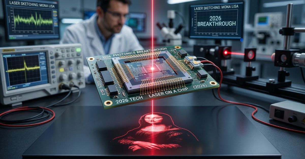
What Is the “Laser on a Chip” Technology?
Researchers have created a microscopic device that can launch and scan laser beams directly from a semiconductor chip. The technology uses a tiny structure called a photonic “ski-jump” waveguide that bends upward from the chip surface.
This structure allows a beam of light traveling inside the chip to exit into open space and move rapidly across a surface.
Because the device is extremely small—smaller than a grain of sand—it can be integrated directly into photonic circuits used in advanced computing and sensing systems.
The team demonstrated the system by sweeping a laser beam across a surface thousands of times per second to create images. Among the images produced was a recognizable sketch of Leonardo da Vinci’s Mona Lisa, showing how precisely the beam can be controlled.
How Scientists Used the Laser to Draw the Mona Lisa
To demonstrate the concept, the researchers used the tiny scanner to trace patterns with light.
The device vibrates very rapidly when electrical signals are applied. As it moves, the tip of the structure directs the laser beam in different directions. By adjusting brightness and motion, the beam can draw patterns and images.
During lab tests, the system produced several shapes and logos, including a A Laser on a chip can monalisa sketch, by rapidly scanning the beam across a surface.
The process is similar to how a laser projector creates images, but here everything happens on a microscopic chip.
Why This Technology Is Important
The real innovation is not the artwork but the ability to connect optical chips with the physical world.
Modern photonic chips can control light extremely well inside tiny channels. However, sending those light signals out of the chip and into open space has been difficult.
This new design provides a direct pathway for light to exit the chip and scan across space.
Experts say this could enable several advanced technologies:
- Smaller and cheaper LiDAR sensors used in autonomous vehicles
- Compact augmented-reality displays
- High-speed optical communication systems
- Precise laser control for quantum computing experiments
The technology may also allow optical systems to generate millions of beam spots per second, far faster than many existing scanning methods.
How the Tiny Device Works
The device is built using standard A Laser on a chip can monalisa sketch manufacturing methods, similar to those used to produce computer chips.
Key features include:
- A silicon-nitride waveguide that carries the laser light
- A microscopic cantilever structure that bends upward
- Piezoelectric materials that vibrate when voltage is applied
When electrical signals drive the structure, it oscillates rapidly. This motion sweeps the A Laser on a chip can monalisa sketch beam across a surface, enabling it to trace shapes or images.
Because the device has extremely low mass, it can move very quickly and precisely.
Current Limitations of the Technology
Although the results are promising, the technology is still in an early experimental stage.
At the moment, the device works best in vacuum environments, where air resistance does not slow its motion. Researchers will need to develop compact vacuum packaging to make the system practical.
Another limitation is that the beam follows repeating scanning patterns. Future designs may need arrays of many devices to allow full control over beam positioning.
Despite these challenges, scientists believe the concept could eventually scale to large optical systems capable of producing billions of laser beam points per second.
Why This Matters for India and the Global Tech Industry
Advances in photonics are becoming increasingly important for global technology development. Countries including India are investing heavily in areas such as quantum computing, semiconductor design, and optical communication.
Innovations like laser-on-chip systems could play a role in:
- Next-generation sensing for smart infrastructure
- High-speed optical networks
- AR and VR technologies
- Future quantum computing platforms
As India continues to expand its semiconductor and deep-tech ecosystem, such technologies may become increasingly relevant for research and industry.
What Happens Next?
Researchers are now working on improving the stability and scalability of the device. Future work may include:
- Integrating multiple laser emitters on a single chip
- Developing compact packaging for real-world applications
- Improving beam control for more complex optical systems
If successful, this technology could lead to extremely compact light-based systems for sensing, computing, and communication.
FAQ(A Laser on a chip can monalisa sketch)
What does “laser on a chip” mean?
It refers to a microscopic device built on a semiconductor chip that can generate and control laser beams directly from the chip surface.
Why did scientists draw the Mona Lisa with a laser?
The Mona Lisa sketch was used as a demonstration to show how precisely the laser beam can scan and create patterns.
What is a photonic chip?
A photonic chip uses light instead of electricity to process and transmit information through tiny optical waveguides.
What technologies could use this invention?
Potential applications include LiDAR sensors, augmented-reality displays, optical communications, and quantum computing systems.
Is the technology available commercially yet?
No. The device is currently in the research stage and still requires further development before real-world use.